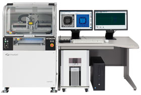
FineSAT Ⅴ
(equipped with the option in the photograph)
The “FineSAT series” is offered as non-destructive equipment for detecting and imaging microscopic structures or defects inside semiconductors and electronic components by use of the reflection and transmission properties of ultrasonic waves.
In response to increasingly sophisticated needs in recent years, we developed “FineSAT Ⅴ” by enhancing the functions of the conventional equipment “FineSAT Ⅲ” and enabling measurement and inspection at improved precision and speed.
“FineSAT Ⅴ,” equipped with independently-developed data processing software and a newly-adopted 64-bit processing system, combined with a high-speed, high-precision scanner, shortens inspection/analysis time.
Ultrasonically measured data of up to 400 million points in standard specification and up to 2 billion points in optional specification *1 can now be stored and processed.
With FineSAT Ⅲ, the minimum measuring pitch was 40 µm when imaging an 200mm (8-inch) wafer in single measurement.
In contrast, FineSAT Ⅴ can obtain and image data in 20 µm pitch in standard specification and in 10 µm or smaller pitch in optional specification, enabling detailed measurement of a large sample in a single scan.
It also enables various image displays that support high-precision analysis/evaluation.

When measuring a large sample such as a wafer, the measurement time is largely affected by the scanning speed. The measurement time of FineSAT Ⅲ is shortened by 25% *2 by reducing the ultrasonic pulse generation cycle by half in addition to using a high-speed scanner. The maximum scanning speed of the scanner excluding acceleration and deceleration time has improved to 2,000 mm/s. *3 The newly designed highly-rigid frame suppresses equipment vibration, producing crisp images even from high-speed scanning.
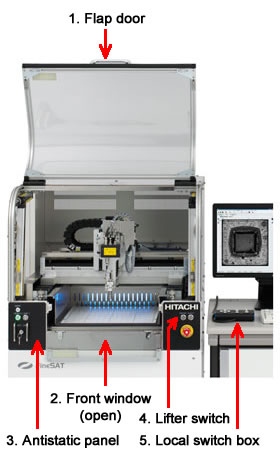
A 64-bit processing system is used to sharply enhance the analytical functions.
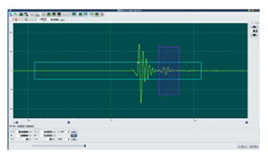
The unit of ultrasonic measuring time can be set to one quarter that of the conventional unit, increasing the depth-direction resolution by 4 times. This improves the detection of delamination or defects inside the thin layers of increasingly fine-processed, multi-layered electronic devices. It also improves the accuracy of depth position information.
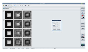
This function is for scanning whilst continuously changing focus points. It enables you to capture images focused at multiple varying depths in a single measurement, thus preventing defects from being overlooked.
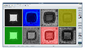
Images obtained from multi-gate measurement, which involve various information, can be displayed in thumbnail view for easy selection.
The color palette of a thumbnail image can be changed individually.
Two images captured simultaneously by reflection and transmission methods of measurement can be overlaid in display.
In addition, the transmission ratio of a displayed image is adjustable, allowing you to choose a setting that provides ease of judgment.
The advanced analytical software that can be used in combination includes: image sharpening software to sharpen images by supplementing the degradation of ultrasonic signals; volume image software to analyze recorded waveform data into measured images and waveforms after measurement; and void viewer software to display voids (defects) and make acceptance/rejection judgment and perform statistical processing.
| FSP8Ⅴ | FSP12Ⅴ | |
| Probe frequency (MHz) | 5–200 | 5–400 |
| Effective stroke (X × Y × Z) (mm) | 350 × 350 × 80 | |
| Maximum scanning speed (mm/s) | 2,000 [Nominal value] | |
| Maximum measurement counts (points) | Standard: 400,000,000 GUIPC option: 2,000,000,000 |
|
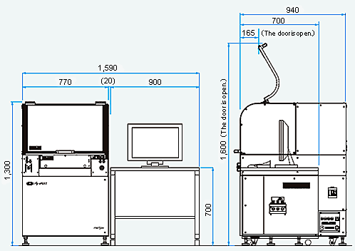
| External dimensions (W × H × D) (mm) | 1,590 × 1,300 × 940 (with the door closed) | |
| Mass (kg) | Approx. 470 | |
| Power supply (voltage/current/frequency) | AC100V/15A/ 50/60 Hz | |
(Unit: mm)
